If you’re familiar with the Japanese art of paper folding — origami — you probably already know that with a few carefully executed folds, you can create just about anything. There’s a good chance, though, that this particular concept from researchers at the University of Chicago will blow you away like a sheet of paper in the wind: creating 3-D electronic circuits based on the principles of origami.
Origami and originality
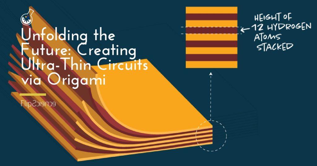
Jiwoong Park and his colleagues used anatomically thin materials to synthesize large-scale integrated circuits. These origami-style circuits, in turn, form a 2-D module when laterally stitched together. In a simple but innovative twist, Park and his team vertically integrated the 2-D modules, creating 3-D stacks.
The integrated circuits found in today’s gadgets consist of silicon and bulky substrate platforms. Until recently, they did not have the capacity to function independently. The use of anatomically thin materials handily bypasses these limitations. Furthermore, the use of multiple ultra-thin “building blocks” enables the incorporation of different electric and thermal properties into the circuit. This allows the circuit’s functionality to increase exponentially.
As Park explained:
“For our research, we first generate atomically thin paper with different color[s] representing different electrical, optical, or thermal properties. We combine them in the lateral direction, equivalent to stitching. We stack them on top of one another, which is vertical integration. By doing so we are trying to develop large scale, fully functioning integrated circuits using these atomically thin materials as 2-D building blocks or color paper.”
As and added bonus, the resulting circuit is smaller, but not too small for the naked eye to see. This is due to the manner in which the 2-D components are arranged; you wouldn’t even need anything more complex than an ordinary optical microscope to handle it without fear.
A good idea — and not just on paper
Thanks to this origami circuit concept, a ton of new innovations in everyday life just might be possible. From the incorporation of these ultra-thin chips into umbrellas or parachutes to the creation of an entirely new line of devices with condensed circuitry, the possibilities seem limitless. As Park elaborates:
“What we are interested in developing is this mechanism of taking all these surfaces and device elements and folding them into tight spaces. Upon our cue, we want them to deploy to really large functioning surfaces.”
Park presented his team’s findings, including the details of their circuit construction and its potential applications, at the AVS 64th International Symposium & Exhibition last Nov. 1 in Tampa, Florida.

Author: Mikael Angelo Francisco
Bitten by the science writing bug, Mikael has years of writing and editorial experience under his belt. As the editor-in-chief of FlipScience, Mikael has sworn to help make science more fun and interesting for geeky readers and casual audiences alike.


